
SEMICONDUCTOR / PCB / PRECISION ASSEMBLY
Wafer and PCB warpage measurement starts with the datum
A height map becomes useful only when its reference plane, support condition and scan coordinates are defined. Treat an opaque PCB, a polished wafer and a transparent layer stack as separate optical jobs.
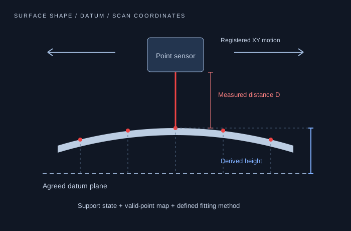
Define which surface and which shape result you need.
Warpage, local step height, runout and thickness variation answer different questions. Specify the report definition before selecting a sensor.
| Part and task | Technology to assess | Key boundary |
|---|---|---|
| Opaque PCB surface height | TRI / PRO point scanning; 2D profiles where the field and finish permit | Copper, solder mask, component edges and holes require a valid-point policy |
| Polished wafer surface map | Specular-capable point arrangement; confocal or full-field method review | A diffuse-only return arrangement may miss the reflected beam |
| Transparent layers or surface discrimination | Confocal / layer-sensitive optical review | Wavelength alone does not identify the required interface |
| Thickness variation or mid-surface shape | Two-sided measurement and a defined calculation method | One front-face height map does not establish thickness or mid-surface warp |
Keep the fixture state in the result definition.
Record whether the part is free, supported at specified locations, vacuum-chucked or clamped. A fixture can flatten the part or introduce a new shape, while a thin wafer or flexible PCB can sag under its own weight between supports. Use the same support, orientation, temperature and settling time when comparing the optical result with a reference method.
Define a datum from specified points or an agreed fitting method. Removing a best-fit plane removes rigid tilt; the remaining deviation still depends on the selected area and excluded features. Do not label a generic peak-to-valley surface result as a standards-compliant wafer bow, warp or flatness result without the required definition.
Turn distance readings into a registered height map.
A stationary point sensor returns one local distance. A surface map requires known XY motion or multiple measurement positions. Log encoder positions and acquisition times, then convert calibrated distances to height in the agreed coordinate system. Stage straightness, pitch and fixture motion can appear in the map.
Set the scan pitch from the smallest feature that must be resolved, not from the output resolution. State which pads, vias, edges, holes and component regions are included or masked. Keep a coverage map alongside the height map so missing readings are distinguishable from a flat surface.
For a 2D line scanner, one profile is a cross-section. Adding a controlled motion axis can build a surface map only if profiles are registered to motion. Check the usable X field at both Z extremes and define stitching where more than one pass is needed.
Review reflective and transparent wafers separately.
For a polished wafer, assess the incidence angle and available receive path across the complete scan. A valid reading at the center does not establish valid return at a bowed edge. Supply representative finish, coatings and expected slope to select the measurement arrangement.
Confocal and deflectometry are distinct alternatives used for different semiconductor tasks. The linked manufacturer overview illustrates this diversity. An LDS-CNF interest request initiates a technology review; it does not describe a released product or guarantee a transparent-layer measurement.
BEFORE THE PURCHASE ORDER
Validate the map with the fixture and stage included.
Freeze the definition
Specify support points, datum method, edge exclusion, valid region, temperature and output statistic. Keep original coordinates and masks with the report.
Separate stage from part
Scan a suitable reference artifact using the same motion path. Investigate stage and fixture contributions before assigning all deviation to the part.
Repeat the handling cycle
Unload and reload representative parts and compare maps at the same coordinates. Distinguish measurement repeatability from fixture and handling variation.
Check the difficult areas
Include reflective regions, solder-mask changes, edges and expected maximum slope. Agree allowable missing-data coverage and comparison with the reference method.
These are proposed validation steps. They do not represent completed testing, a calibration certificate or a performance commitment for an LDS configuration.
HARDWARE / INSTALLATION REFERENCE
Review target access as carefully as the sensor housing.
Define the target surface, scanning motion and datum first. These point-sensor views are installation references, not wafer-test results.
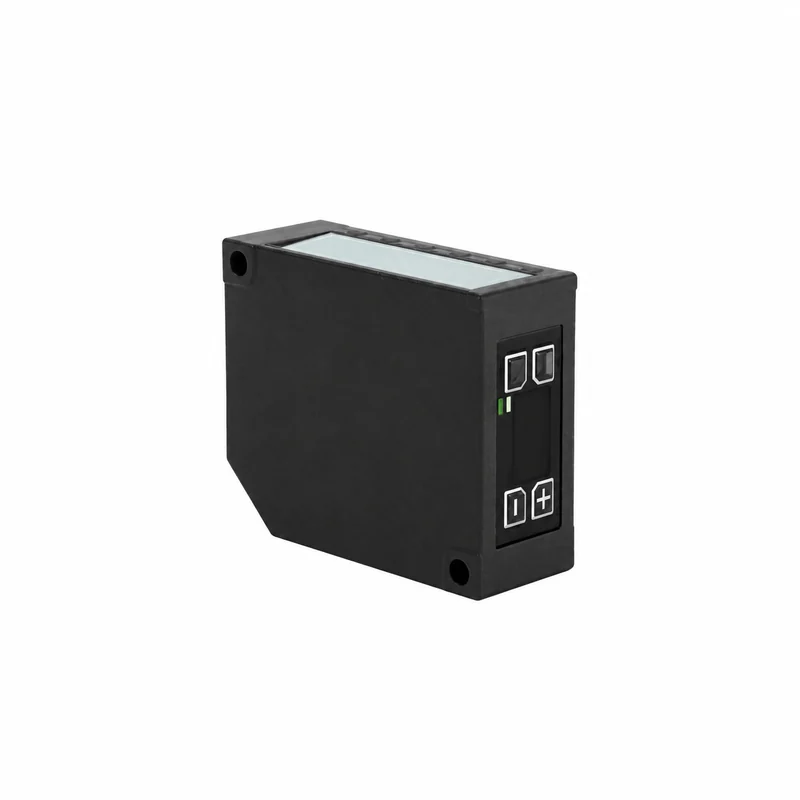
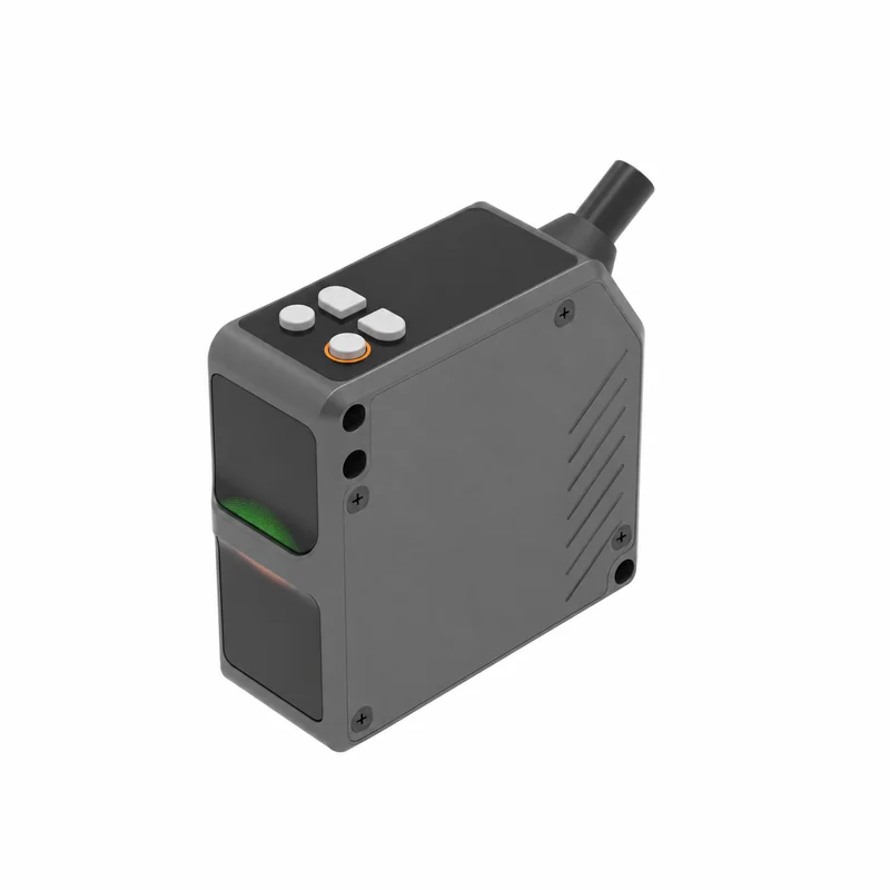
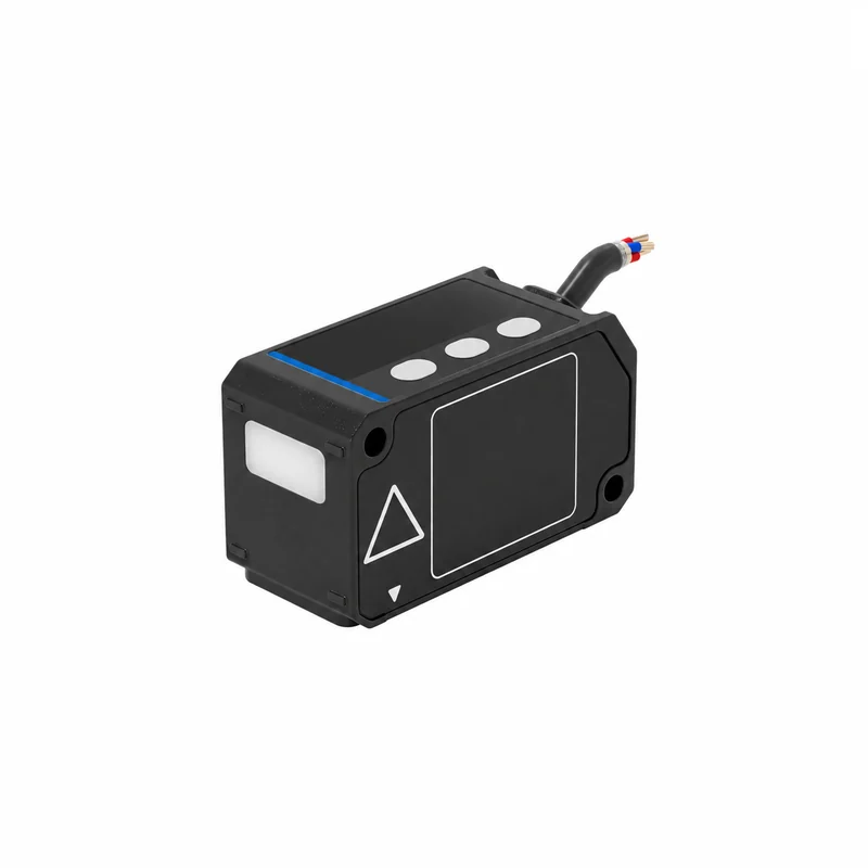
Representative housing views. Confirm the exact model, dimensions and supply scope. Housing color does not identify laser wavelength.
Compare the sensing options for this task.
Sub-micron high-speed laser displacement gauges
10±2 to 150±40 mm requests
Review configuration and integration ↗Request LDS-PRO for this application ↗CMOS laser displacement sensors
25–1,000 mm distance requests
Review configuration and integration ↗Request LDS-TRI for this application ↗2D laser profile sensors & line scanners
Z: 10–600 mm · X: 15–500 mm requests
Review configuration and integration ↗Request LDS-2D for this application ↗Questions before you specify the system
Can one laser displacement sensor measure wafer warp?
A point sensor can contribute local heights to a scan. A useful warp or surface-shape result also needs motion coordinates, a datum, a support definition and a calculation method. One local reading does not describe a whole wafer.
Does blue light make every wafer measurable?
No. Reflectivity, transparency, layer structure and incidence angle determine the usable optical return. A specular arrangement or another optical principle may be needed; test representative parts.
Is front-face flatness the same as total thickness variation?
No. A front-face map includes the effect of support and surface shape. Thickness variation requires information about both faces or a method that resolves the relevant interfaces.
Wafer & PCB warpage / ENGINEERING HANDOFF
Send the process conditions with the request.
Wafer or PCB dimensions; surface finish and layers; supported, clamped or free state; scan area and grid; datum method; temperature; allowable height deviation; cycle time.
Include your existing sensor/controller model, required document revisions, quantity and destination. After reviewing the brief, the next step is a proposed configuration and confirmation of the available drawings, integration information and test scope before a formal quotation.
The form retains this application-page context. Confirm the actual family and range for your machine. For confidential drawings, agree an NDA and transfer method before sending files.
Prepare the drawings, data and acceptance scope.
Laser Sensor PLC Integration Guide
Confirm the ordered hardware, wiring drawing and data semantics together. An M12 connector or an Ethernet port describes only part of the integration.
Open the engineering checklist ↗Laser Sensor Calibration Review
Start with the quantity you need to accept, the conditions under which it is measured and the evidence that belongs to the delivered unit or complete system.
Open the engineering checklist ↗Laser Sensor Safety & Compliance
Prepare one review package for the ordered head, its optical variant and the machine around it. Start with identifiable documents and the access conditions your EHS team needs to assess.
Open the engineering checklist ↗